Newsletter
Stay up to-date with the latest imaging, analysis and metrology news from Digital Surf.
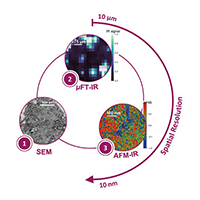
The AFM-IR lab at the Institute of Physical Chemistry, Paris-Saclay University (Orsay, France) is the pioneering research group in Infrared-Atomic Force Microscopy (AFM-IR). In particular, the team specializes in the characterization of complex materials, ranging from astro to biosciences, including studies on pathological calcifications such as breast microcalcifications (MCs), described in this article by Margaux Petay, former AFM-IR lab PhD student.
Simone Ruggeri, Associate Professor leading the Nanoscale Microscopy and Spectroscopy group at Wageningen University (WUR), Netherlands, tells us more about his current projects in the development of nano-analytical imaging and spectroscopic technologies to open a new research window of observation with nanoscale sensitivity in chemistry, biology and materials science.
Strain in semiconductor devices can be used to influence the electronic properties, and is used as so in strain engineering. Renata Lewandowska, product manager for spectral applications at Digital Surf, explains why Raman spectroscopy is an ideal technique for measuring strain, and give us an example.
Application experts at Horiba Scientific and JEOL Europe recently highlighted a technique for precisely relocalizing specific areas of a sample for analysis using various techniques including Raman microscopy, scanning electron microscopy (SEM) and energy dispersive spectroscopy (EDS).
The Institute of Electronics, Microelectronics and Nanotechnology (IEMN) in France recently completed the “Dirac III-V” project investigating ways of producing Dirac electrons (electrons without any mass). This project called for the use of many different fabrication methods as well as a software program capable of bringing together and processing the different kinds of datasets generated.
For this application, a research team at the LNE Nanotech Institute combined measurements from several instrument techniques including Atomic Force Microscopy (AFM) and Scanning Electron Microscope (SEM) equipped with a new-generation energy dispersive X-ray detector (EDX). They used MountainsLab® software to correlate the collected data and extract the relevant information.
Tailoring 2D semiconductor heterostructures with specific bandgaps is a key aspect of leveraging new quantum materials for electronics and optoelectronics, one of the hot topics for researchers currently working in nanotech. Craig Wall, applications scientist at Montana Instruments, recently investigated the subject using Mountains® software to analyze results from Raman spectroscopy and photoluminescence.
Scientists from the ISEN (Institut Supérieur de l’Électronique et du Numérique) in Lille, France, used photoelectron spectroscopy to investigate a new method for growing PbS nanoplatelets on InP surfaces.
Bruno Grandidier, research scientist with the French National Center for Scientific Research (CNRS), reports on his work, focused on understanding the electronic properties of silicon dangling bonds.
Researchers at L'Oréal use Raman imaging to study the physicochemical properties of sunscreen to better understand the distribution of UV filters.
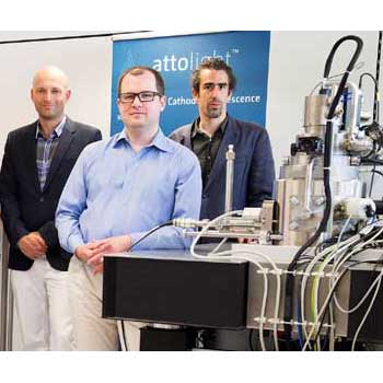
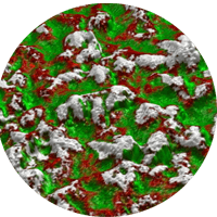
Quantitative cathodoluminescence technology coupled with the power of Mountains® software made it possible to localize and identify degraded layers in state-of-the-art green laser diodes.