By Claire Kayser, Product Manager for Profilometry at Digital Surf

As electronic devices continue to shrink while increasing in complexity, ensuring the reliability of interconnections has become a critical challenge for manufacturers. In semiconductor packaging, particularly in ball grid array (BGA) packages and other high-density assemblies, small geometric deviations can have significant consequences on performance and durability.
Two parameters are especially critical: coplanarity and warpage.
Coplanarity refers to the relative height of solder ball terminations. For a reliable electrical connection, all solder balls must make uniform contact with the PCB. Even slight variations can result in weak or intermittent connections.
Warpage, on the other hand, describes the deformation of the substrate, often caused by thermal cycles and mechanical stress during manufacturing processes such as reflow soldering. Excessive warpage can prevent proper contact altogether, leading to immediate or latent failures.
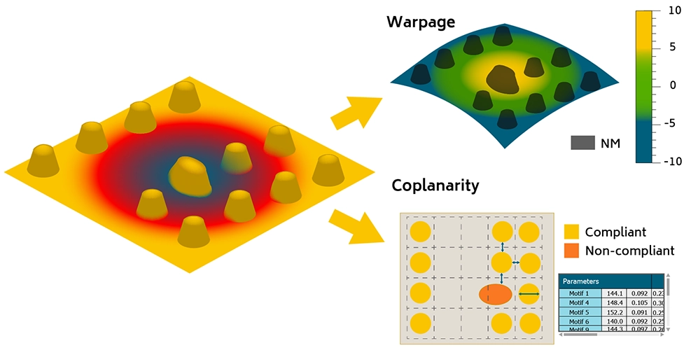
Above. Warpage and coplanarity can have a critical impact on the reliability of electrical connections.
These issues are not limited to semiconductor manufacturing. They are equally relevant in high-reliability sectors such as aerospace, medical devices and defense electronics, where failure is not an option.
From visual inspection to quantitative analysis
Traditionally, inspection methods have relied on visual checks or limited measurements, which can be time-consuming and insufficient for detecting subtle defects across large arrays of components. As assemblies become more complex, there is a growing need for automated, quantitative approaches capable of analyzing entire datasets with consistency and precision.
Modern surface metrology solutions now enable engineers to go beyond simple observation. Using 3D surface data, it is possible to measure substrate deformation, calculate coplanarity across hundreds or thousands of solder balls and identify deviations with micrometer-level accuracy.
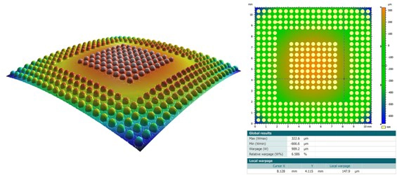
Above. Substrate deformation (warpage) visualized using 3D surface metrology.
These tools also allow for the detection of common defects such as bridging between solder balls, misalignment and irregular geometries. By combining geometric analysis with statistical evaluation, manufacturers can establish clear acceptance criteria and quickly determine whether a component meets specifications.
Early defect detection for better process control
One of the key advantages of advanced coplanarity and warpage analysis is the ability to detect defects early in the production process. This has a direct impact on yield and cost.
Short-term risks such as short circuits, overheating or functional failures can be mitigated before assembly. At the same time, long-term reliability issues, often caused by mechanical stress or uneven contact, can be significantly reduced.
Automated workflows further enhance efficiency by enabling fast, repeatable analysis.
In some cases, AI-assisted detection can help identify patterns or anomalies that might otherwise go unnoticed. This not only saves time but also improves consistency across inspection batches.
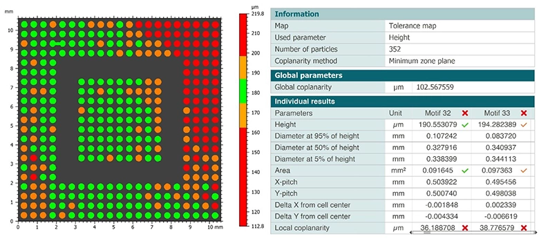
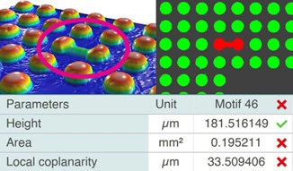
Above. Coplanarity: use AI-assisted structure detection, set tolerance limits for key parameters and visualize maps of pass/fail statuses.
Integrating analysis into industrial workflows
To be effective, these capabilities must integrate seamlessly into existing production and quality control processes. This includes the ability to define tolerances, apply pass/fail criteria, and generate traceable reports for process monitoring and compliance.
Above. Define pass/fail criteria to highlight defects such as bridging.
Beyond measurement and detection, robust analysis also relies on the ability to structure and organize data consistently. In the case of ball grid array components and similar assemblies, this often involves defining a regular grid of features and assigning a stable index to each termination. Such indexing ensures that each solder ball can be tracked and compared across multiple samples, even in the presence of misalignment, missing elements or local defects. This is particularly valuable for identifying recurring issues affecting specific locations within the array.
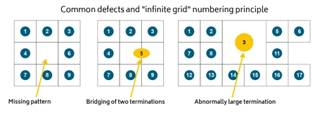
Above. Stable indexing of terminations allows consistent tracking of each structure even in the presence of defects.
In practice, these grids can adapt to real-world conditions: they may be rotated, non-orthogonal or based on rectangular patterns, while still maintaining consistent indexing. When a regular grid cannot be established due to highly irregular distributions, meaningful analysis remains possible, with key parameters such as height, local and global coplanarity, area and diameter still accessible.
Solutions such as MountainsMap® software provide dedicated tools for coplanarity and warpage analysis, allowing users to combine advanced surface metrology with intuitive visualization and reporting tools. MountainsMap® also ensures engineers have constant access to the latest standardized parameters (ISO, JEDEC), allowing them to guarantee compliance with industry specifications.
Towards more reliable electronic systems
As electronic assemblies continue to evolve, controlling geometric parameters at every stage of the process is becoming essential. Coplanarity and warpage analysis provide a powerful means to improve both immediate performance and long-term reliability.
By moving from reactive inspection to proactive process control, manufacturers can reduce risk, improve yield and meet the increasing demands of modern electronics.
Try Coplanarity & Warpage Analysis on your data now
Learn more about
Author : Claire Kayser