Newsletter
Stay up to-date with the latest imaging, analysis and metrology news from Digital Surf.
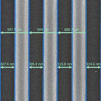
In the semiconductor industry, precise characterization of nanostructures is essential to ensure device performance and reliability. Line Edge Roughness (LER) and Line Width Roughness (LWR) play a critical role in process control. Mountains® software provides a dedicated solution for accurate, automated and robust LER measurements, ensuring reliable results regardless of imaging conditions such as accelerating voltage.
The semiconductor industry relies on uncompromised metrological precision. The optimal exploitation of AFM data requires powerful and adapted software, capable of transforming raw data into actionable insights. This is where Mountains® software comes into play, offering a high-performance solution for the precise and efficient analysis of Critical Dimensions (CDs) in the semiconductor field.
Strain in semiconductor devices can be used to influence the electronic properties, and is used as so in strain engineering. Renata Lewandowska, product manager for spectral applications at Digital Surf, explains why Raman spectroscopy is an ideal technique for measuring strain, and give us an example.
Researchers at the Institut de Ciència de Materials de Barcelona characterizied surface texture of superconductor materials with the aim of improving their performance.
The Institute of Electronics, Microelectronics and Nanotechnology (IEMN) in France recently completed the “Dirac III-V” project investigating ways of producing Dirac electrons (electrons without any mass). This project called for the use of many different fabrication methods as well as a software program capable of bringing together and processing the different kinds of datasets generated.
Scientists from the ISEN (Institut Supérieur de l’Électronique et du Numérique) in Lille, France, used photoelectron spectroscopy to investigate a new method for growing PbS nanoplatelets on InP surfaces.

Nanolithography is a precise patterning technology used to fabricate functional nanostructures for applications in biosensors, advanced materials and extensively in the semiconductor sector for solar cells, printed electronics, LED, MEMS, etc.
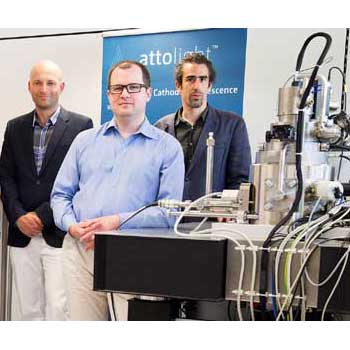
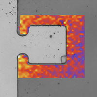
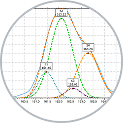
Quantitative cathodoluminescence technology coupled with the power of Mountains® software made it possible to localize and identify degraded layers in state-of-the-art green laser diodes.