In advanced electronics manufacturing, even the smallest surface deviation can lead to major reliability issues. This is especially critical in ball grid array (BGA) packages, chip carriers, and other semiconductor packaging technologies used for integrated circuits.
The Coplanarity & Warpage Analysis module for Mountains® software helps you confidently control assembly quality, from die-level analysis to full package inspection, ensuring optimal electrical contact and long-term product performance.
Built for industry and research
- Ideal for:
- Semiconductor packaging and PCB manufacturing
- Inspection of BGA packages and ball grid array components
- High-reliability industries (aerospace, medical, defense)
- R&D and materials analysis labs working on integrated circuits and die characterization
- Flexible workflows adapted to your specific applications
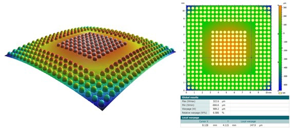
Above. Reveal substrate deformation and identify critical zones instantly with 2D & 3D warpage visualizations.
Control critical assembly parameters
- Measure substrate warpage caused by thermal and mechanical stress in semiconductor packages
- Verify coplanarity of solder balls (or bumps) in ball grid array (BGA) packages for optimal PCB contact
- Evaluate geometry and positioning of chip carriers and IC packages using the latest ISO / JEDEC parameters
- Automatically structure arrays using grid-based analysis with consistent indexing of each termination, enabling reliable comparison across samples, even in the presence of misalignment or missing elements
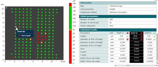
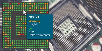
Above. Coplanarity: set tolerance limits for key parameters and visualize map of pass/fail statuses.
Identify defects early
- Automatically or semi-automatically detect:
- Bridging (short circuits between solder balls or bumps in BGA packages)
- Misalignment in chip carriers and substrates
- Non-conforming solder balls (size, shape or uniformity deviations) affecting integrated circuit connections
- Reduce risks such as:
- Electrical failure
- Overheating
- Long-term reliability issues in semiconductor devices
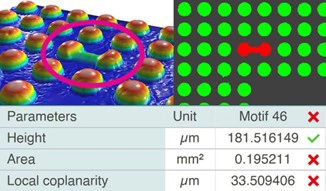
Above. Highlight defects such as bridging and define pass/fail criteria.
Gain time with automation
- Fast, repeatable analysis workflows for semiconductor inspection
- Configurable automation for industrial packaging and assembly environments
- Optional AI-assisted detection of BGA and die-related defects
- Easy integration into production and inspection processes
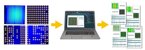
Above. Save time by easily automating coplanarity and warpage analysis of large datasets.
Make confident decisions
- Define tolerances with pass / warning / fail thresholds for BGA and IC assemblies
- Visualize results with clear color maps of coplanarity and warpage
- Generate statistical analysis for full traceability in semiconductor manufacturing
- Combine multiple criteria for advanced quality control of integrated circuit packaging
- Track and compare individual terminations across datasets thanks to stable indexing, supporting automated quality control
Available as an optional module with:
- MountainsMap® Imaging Topography
- MountainsMap® Expert
- MountainsMap® Premium
- MountainsLab® Expert
- MountainsLab® Premium