Nanowires (NWs) are of great interest for their useful electrical, electromechanical and thermoelectrical properties and, in past decades, many R&D efforts have focused on their development. In this study, an inter-laboratory comparison of AFM dimensional and surface roughness characterization on silicon NWs, involving different national metrology institutes in Europe, is reported by researchers Alexandra Delvallée and Luigi Ribotta. The work was led by the Nanometrology and Surface Metrology group at INRiM, the Italian National Metrology Institute, which has several decades of experience in quantitative analysis at the nanoscale.
A protocol for nanodimensional measurements with AFM
Nanometrology plays a crucial role in ensuring the traceability and reliability of measurements through the development of methods specifically tailored to instrumentation at the nanoscale. The use of multiple, well-assessed characterization methods is a growing and essential practice to enable a broader comprehension of structural, physico-chemical and functional properties of nanomaterials.
As well as providing the roughness properties of the wires, with their uncertainties evaluation, the results of this study also helped demonstrate the comparability of the measurement results obtained with various instruments.
The diameter and roughness parameters are extracted as explained in the caption of Figure 1. Experimental data shows good consistency, with a standard deviation of 15% relative to the mean top-height diameter. Moreover, combined standard uncertainties given are included in a range from 2.2% to 2.9%.
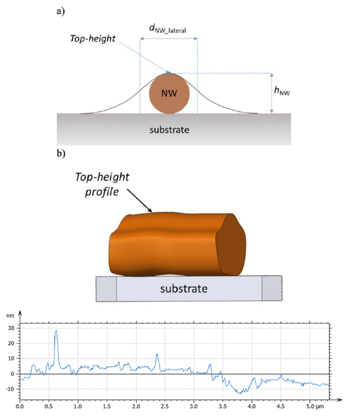
Figure 1 (a) Cross section of a nanowire deposited on a surface. The gray line is a profile achieved by the tip: the lateral diameter (dNW_lateral) is enlarged by convolution between the tip and the NW. The diameter can be extracted from the height of the NW hNW. The height of the nanowire is defined as the vertical distance between the ‘top height’ and the substrate. (b) Along the total length diameter, variations of a few nanometers can occur due to the continuous immersion in the etching solution during fabrication. Because of this, the top-height point had to be extracted on several profiles along the NW, ideally on each line of the AFM image. As a result, a profile all along the NW can be determined and can also be used to determine the roughness parameters all along the NWs, extracted by using MountainsSPIP® software.
Concerning NW roughness, no standard or guide exists for assessing the uncertainty associated with it. We propose a methodology, based on Monte Carlo approaches and the results are consistent (combined standard uncertainty results ranging from 0.3% to 5.0% for Ra values and from 0.3% to 4.4% for Rq values).
Colocalizing nanowireS measured by different AFMs around Europe
In a recent study led by the LNE (Laboratoire National de métrologie et d’Essais, France), it has been demonstrated that characterization on exactly the same nano-objects using different instruments can reduce measurement uncertainties. The idea here is, using dedicated marked substrates (Figure 2), to locate a region of interest (ROI) and to image these ROIs with the various AFMs of participating European countries.
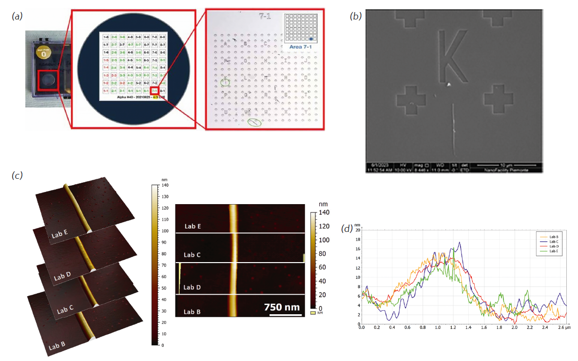
Figure 2 (a) (left) One of the three samples used for the study, (center) schematic view of the different numbered zones on a substrate, (right) optical microscope view of a numbered zone (here zone 7–1) on a marked silicon substrate (9 mm x 9 mm) where nanowires are deposited. The green regions indicate the presence of isolated NWs while the red regions indicate the presence of bundles not approached with the AFM tip. (b) SEM image of an area with NW deposited on marked silicon substrate. (c) Colocalized AFM images of the same nanowire acquired by four different laboratories using MountainsLab® software (d) Comparison of the extracted roughness profiles from the different labs.
Firstly, each image was processed independently, i.e. here leveled. Then, the “Colocalization” tool was used to combine the data from the different images and to ensure that strictly the same area was compared by each European laboratory.
In order to extract the roughness profile from the NW acquired with the AFMs, we used a MATLAB routine integrated into MountainsLab® software to extract the highest point from each line. The results are shown in Figure 2 (d). The mean trough Ra value the different laboratories measured was 0.7 nm with a standard deviation of 0.2 nm.
Instruments & software used
Atomic Force Microscopy (AFM), Scanning Electron Microscopy (SEM), Transmission Electron Microscopy (TEM), MountainsSPIP® & MountainsLab® software.
Read more
AFM interlaboratory comparison for nanodimensional metrology on silicon nanowires. Luigi Ribotta, Alexandra Delvallée, Eleonora Cara, Roberto Bellotti, Andrea Giura, Ivan De Carlo, Matteo Fretto, Walter Knulst, Richard Koops, Bruno Torre, Zineb Saghi, Luca Boarino. Measurement Science and Technology, Volume 35, Number 10, 2024, doi.org/10.1088/1361-6501/ad5e9f