The constant demand for lower process costs, easier implementation and higher throughput continues to push the development of nanolithography technology.
Besides traditional photolithography, various nanolithography technologies such as electron beam lithography, nano-imprint lithography and nano-sphere lithography have been developed[1][2][3].
After the pattern structure is generated, a precise characterization method is required to quantitatively check the quality of the structure. Since most lithographic patterns have a 3D structure, the characterization technique should offer the capability to measure in 3D.
AFM: the ideal tool for 3D nano-material charactacterization
The atomic force microscope (AFM), which utilizes a sharp probe to scan across the sample surface to record the surface morphology, provides not only high spatial resolution but also high vertical resolution at nanometer and sub-nanometer scale.
In this study, industrial researchers used the new AFM from Anton Paar, Tosca™ 400, equipped with Tosca™ analysis software based on Digital Surf’s Mountains® surface analysis technology to characterize aluminum nanoparticles deposited on indium tin oxide (ITO) coated glass using lift-off based vapor deposition with electron beam lithography.
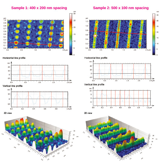
Two different aluminum nanoparticle patterns were deposited on ITO coated glass then imaged by using Tosca™ 400 in tapping mode:
in the first case, a 400 x 200 nm pattern was used for nanoparticle deposition
in the second, a 500 x 100 nm pattern was fabricated.
Surface geometry at the nano-scale
Using Tosca™ analysis software, surface morphology of the Al nanoparticle patterns was analyzed.
Two cross sectional (horizontal and vertical) profiles were extracted from the AFM topography image.
The lateral distance between nanoparticles was quantified by measuring the peak to peak distance. Pattern spacing was easily verified for both samples.
In the second sample, adjacent nanoparticles appeared to have already bonded to each other (or the gap between them was beyond the limit that the AFM tip could resolve). Despite this, spacing between nanoparticles could still be precisely measured. This suggests that 100 nm spacing is not sufficient to clearly separate the nanoparticles based on the deposition conditions.
Getting a better picture of surface structure
In order to see the structure more clearly, the data was displayed in three-dimensional view. Height amplification was applied to help the user see the 3D structures. Nanoparticles in the first sample had clear spacing while those in the second sample had already connected to each other, forming a line (or the gap between nanoparticles may be too small to be resolved).
The height of the nanoparticles in both cases varied from around 15 to 30 nm which suggests that the lift-off mask used in the lithography process may have varied in different locations, resulting in this non-uniform pattern.
References
[1] W. Rechberger, A. Hohenau, A. Leitner, J.R. Krenn, B. Lamprecht, F.R. Aussenegg, Opt. Commun. 2003, 220, 137.
[2] K.J. Byeon, H. Lee, Eur. Phys. J. Appl. Phys. 2012, 59, 10001.
[3] X.Zhang, E.M. Hicks, J.Zhao, G.C. Schatz, R.P.V. Duyne, Nano Lett. 2005, 5, 1503.
Measurements & initial text provided by Dr Ming Wu.
Samples courtesy of Ao.Univ.-Prof. Dr. Joachim Krenn (Nano-optics Group, University of Graz).
Contact: Anton Paar GmbH – support-nsp@anton-paar.com – Tel: +43 316 257 0 – www.anton-paar.com
Instrument & software used
Anton Paar Scanning Probe Microscope (SPM) + Tosca™ analysis software based on Mountains® technology